Product Introduction

Product Introduction
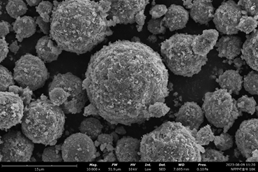
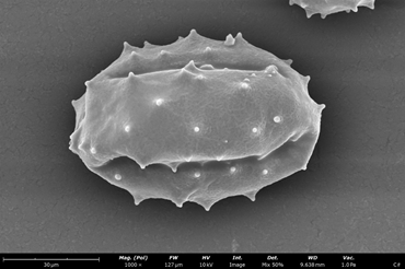
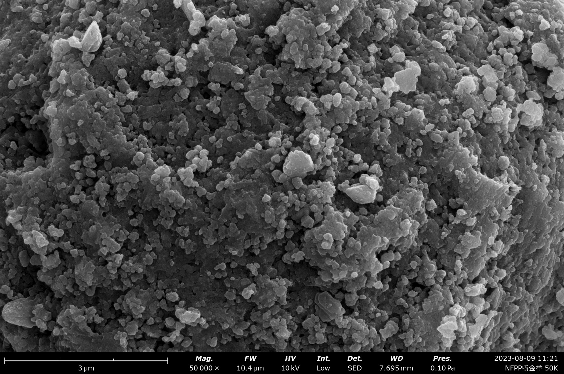
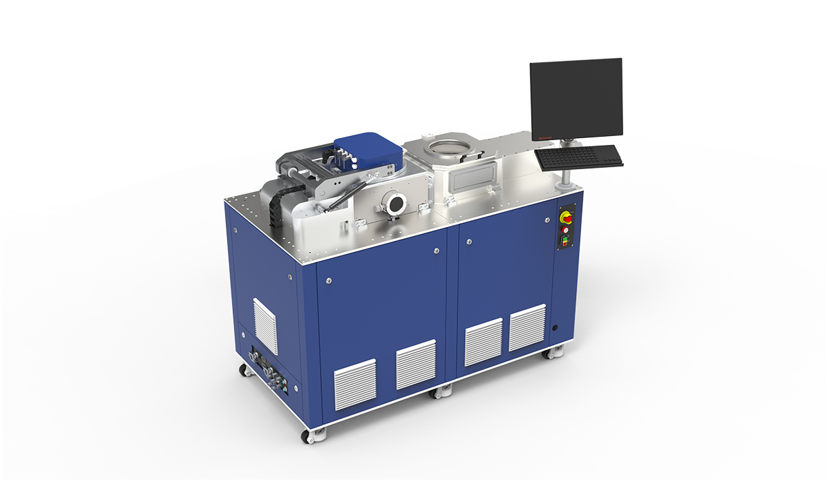
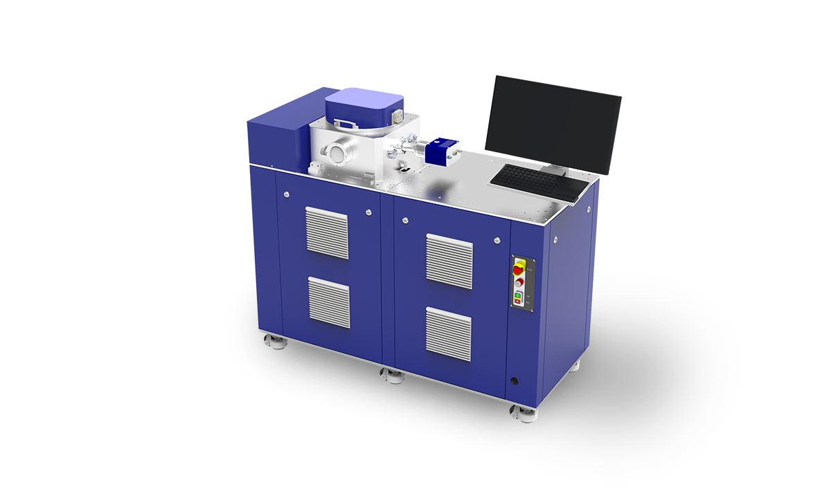
In the past decade, with the optimization of tungsten filaments and electronic circuits, especially the use of compound filaments, the resolution of filament electron microscopes has been further improved, from typical magnifications of several thousand times to several tens of thousands of times, even reaching the level of traditional entry-level field emission microscopes.
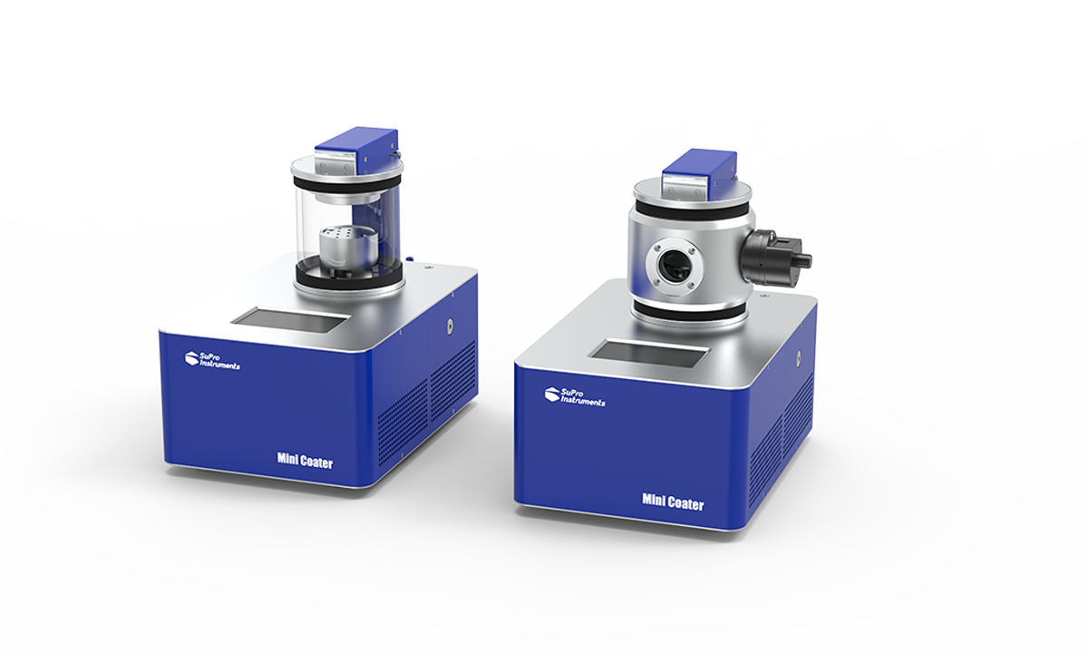
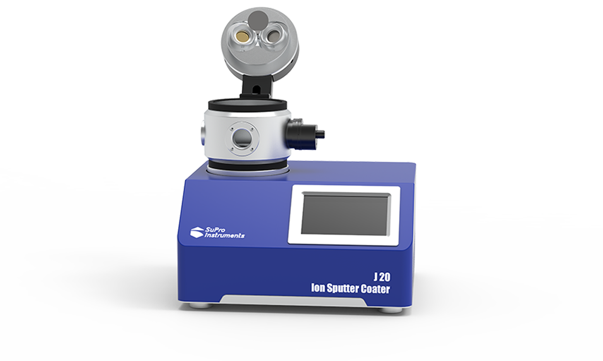
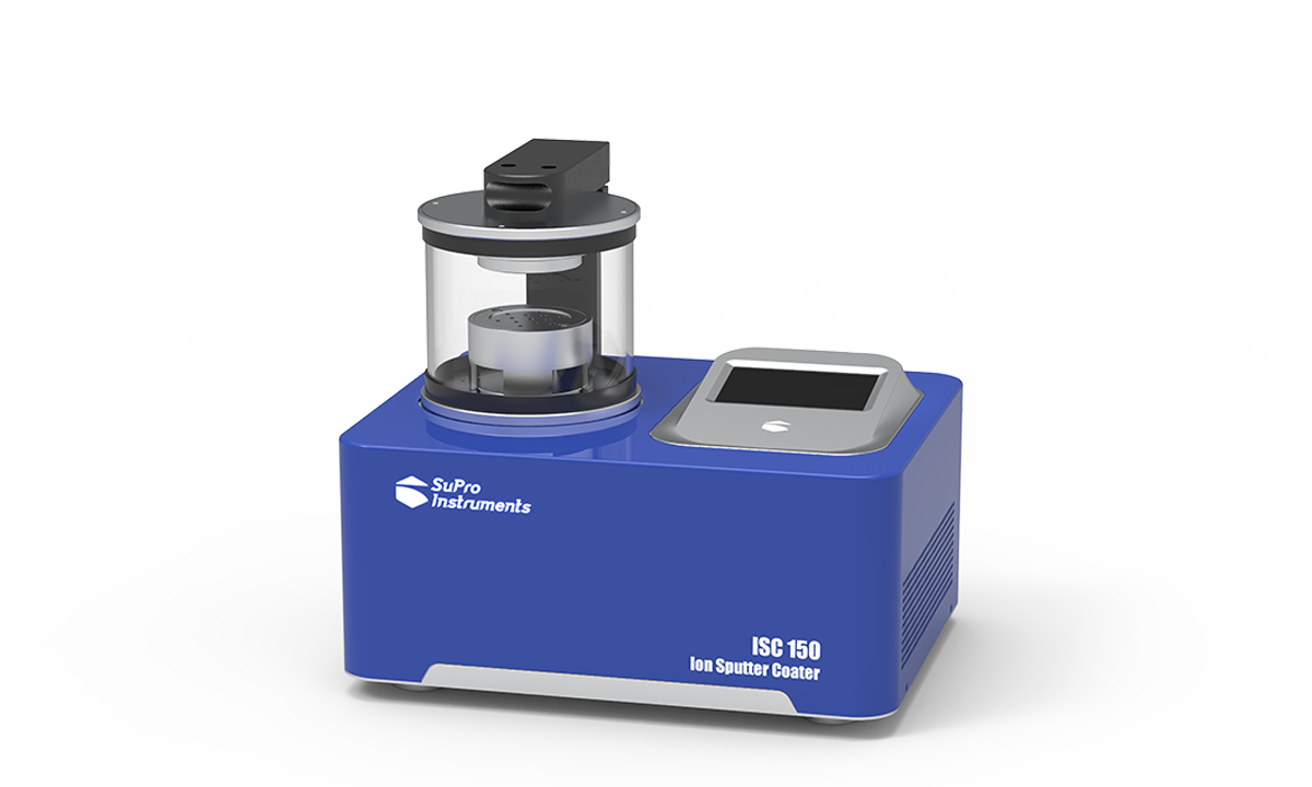
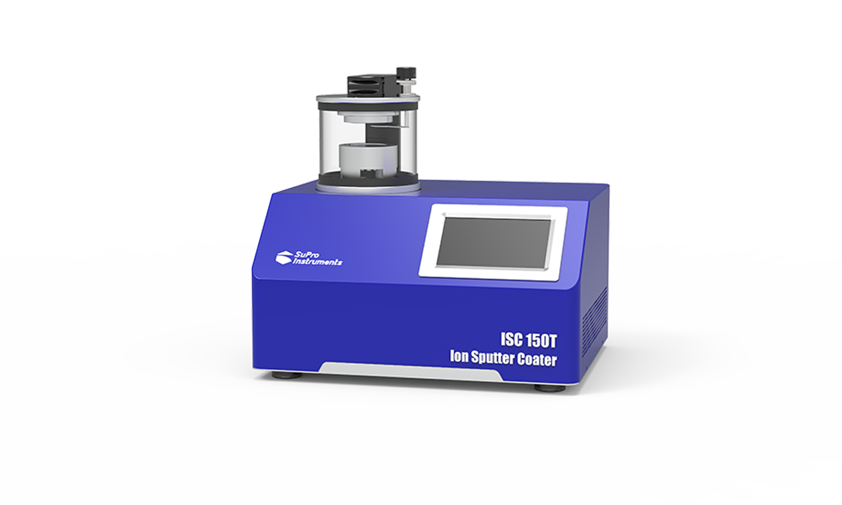
Correspondingly, ion sputtering instruments have also upgraded from diode sputtering to mainly magnetron sputtering. Typically, for magnifications less than 20K times, gold (Au) deposition is mainly used, and in the range of 20K to 100K times, platinum (Pt) deposition is mainly used, which is sufficient to handle most filament SEM scenarios.
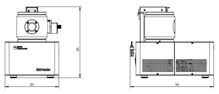
To address the increasing number of 3D sample scenarios (powders, particles, porous materials, fibers, etc.), we have independently designed a digital rotary-tilting sample stage, which ensures more uniform film deposition and enables three-dimensional angular rotation deposition, solving the problem of side coating for samples. It is especially friendly for 3D powder and porous sample SEM preparation.


 EN
EN


 Message consultation
 Appointment for trial

 Product Introduction
